Tagger Microscope
- Main article: Tagger Microscope Contruction (UConn Wiki)
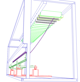
The Tagger Microscope is a movable, high-resolution hodoscope that counts post- bremsstrahlung electrons corresponding to the photon energy band of interest to the experiment in Hall D. While designed as a general-use device, it has been optimized primarily for use in the GlueX experiment, covering the Eγ range of 8.4-9 GeV (Ee 3-3.6 GeV)
In the fall of 2014, the TAGM was installed and it was known that some of the fibers and sub-optimal performance. An updated set of 10 fiber bundles were produced and installed in January 2017. These 10 replaced the lowest yield bundles of the original 17. After analyzing the spring 2017 data, it became clear that the remaining 7 bundles should also be replaced in order to get the highest performance out of the microscope.
In January 2019, the UConn group replaced the remaining 7 bundles making up columns 1..42 with new upgraded bundles, made from fibers with higher photon yield achieved by a combination of better quality control in fusing the scintillating fiber to the light guide and the use of double-clad light guides. This completes the tagger microscope upgrade.
Contents
Focal plane readout scheme
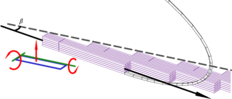
The design of the Tagger Microscope calls for the tagging spectrometer focal plane to be instrumented with an array of scintillating fibers with axes oriented along the direction of the oncoming electrons. Having focal plane segmentation in two dimensions achieves two design objectives:
- fine segmentation along the direction of electrons spread, to maximize the tagging rate per channel and match the energy resolution of the spectrometer;
- segmentation in the y-directions, to match the photon collimator acceptance and achieve acceptable tagging ratios even for small collimator diameters.
To avoid placing photo-sensors along the path of the electronics, the scintillation light is carried via via clear fiber lightguides to a shielded enclosure mounted under the spectrometer magnet, containing the light sensors and readout electronics.
The mechanical alignment structures allows assembly of the scintillating fibers for a wide range of crossing angles (β in the adjacent figure)
Scintillation sensors
The silicon photomultiplier (SiPM) has been identified as the appropriate photo-sensor for reading out the scintillating fibers. Its a novel technology that provides small, pixelated active windows (appropriate to the fiber cross-section) high efficiency and gain with sensitivities to perform single-photon counting at room temperature. It is competitive with traditional PMTs in terms of speed and do not require high voltage to operate (required bias voltages vary between 20-80 V). The solid state sensors are also much less sensitive to magnetic fields, making them a convenient choice for operating next to the tagger magnet.
The tagger microscope design employs custom-designed amplifier boards that can support up to 30 SiPM channels. Each board provides space for mounting the SiPM, initial signal amplification and summation circuitry. The amplifiers are equipped with online-selectable gain-control and online-controllable bias voltages. Thus, uniform quality of readout of all the optical channels can be maintained during run time.
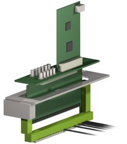
The adjacent rendering shows the amplifier board, mated with "backplane" used to patch signals to the outside of the chamber for readout, as well as the control board (topmost vertical board) which communicates with a computer via Ethernet interface. Bias voltages are set via this interface and various voltages and temperatures at different points of the electronics are queried.
Channel numbering scheme and cable map
For the details of the tagger microscope fiber geometry and the channel numbering scheme, see the following document.
When the microscope readout cable numbering scheme is ordered according to silicon photomultiplier sequence in the TAGM readout, not the order of the fibers on the focal plane. The result of this is a somewhat strange ordering of the column numbers in the data acquisition modules, with column 3 going into the first ADC/TDC channel, followed by columns 2,1, and after that 6,5,4, and so on. This pattern is taken care of in the translation table used to map ADC/TDC channel to detector element, so no one needs to know about it except those who are looking directly at signals at the front end. For the details of the cabling scheme, see the following document.
Custom Electronics and their Readout
Three types of custom electronics were designed for the microscope: the preamplifier, the control board, and the backplane. The preamplifier allows for the readout of the signal from the SiPMs, the control board is the "computer" controlling the microscope, and the backplane carries the signals between boards and the DAQ electronics.
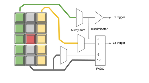
For analyzers, it is important to understand how the microscope preamplifier provides signals. Electronically, all 510 SiPMs can have their signals readout, however, this would require more cables. Instead, every column (5 SiPMs) has the SiPM signals summed into a single output. This is called 'row == 0' in the software. Additionally, 4 columns do have individual readout. These are columns 9, 27, 81, and 99. For these columns, row 1-5 in the software correspond to rows 1-5 of the fibers, where row 1 is closest to the floor and 5 is closest to the ceiling.
Bias Voltages
The power supply for the TAGM only provides a voltage "pool" for the microscope to make use of. It does not immediately bias the SiPMs on the preamplifier. The biases are instead controlled by the TAGM control board which makes use of an FPGA to set the DAC voltages appropriately.
As of 4/2017, the biasing of the microscope is as follows. "No beam" data is taken for three different bias voltages for all 5 rows, taken one at a time while the preamplifier is in high gain mode. This provides an understanding of the SiPM performance, particularly the bias threshold and the gain. Additionally, "beam" data is taken at the same three different bias voltages for all 5 rows, taken one at a time while the preamplifier is in low gain mode. This, combined with the SiPM information, details the performance of the fibers with a predicted yield. This information is stored in a configuration file found in the TAGMutilities directory. For more details about this software package, talk to Richard Jones.
To determine the optimal bias voltage for each SiPM, the configuration file is read in and each column is considered. Within a column, the lowest yield fiber is chosen as the reference. This SiPM is biased according to the user's request, while the remaining 4 SiPMs have their individual bias voltages reduced such that the expected yield matches that of the lowest yield fiber. This produces a uniform pulse height spectrum within the column. However, each column can have a different pulse spectrum. This leads to the need of individual thresholds for the fADC and discriminator, which have been implemented.
The setting of the bias voltages is done through the setVbias command from the TAGMutilities package. Details on this will be kept to the operations wiki page.
Specifications
- Tagger Microscope specification
- File:SiPMspecs.xlsx SiPM specs for all SiPMs in Start Counter, PS and tagger microscope
Microscope Construction
Microscope Fabrication Readiness Review (February 7, 2013)
Light yield tests
slides on light yield measurements
- refractive indices: 1.60 (core), 1.49 (cladding 1), 1.42 (cladding 2, if present)
- mean cosmic yield = (8000 /MeV) * (1.6 MeV/cm) * (mean cosmic scint path length) * (SiPM pde) * (fiber transmission fraction) * (factor for reflection from upstream reflector, if present)
- mean cosmic scint path length = 0.21 mm (from Geant simulation of our setup)
- SiPM pde is 25% in this wavelength range, at the bias levels we are using
- factor for reflection from reflector on end of scintillating fiber was measured to be 1.7 for aluminized mylar
- minimum fiber transmission factor 1.8% needed to meet design goal of 200 pixels per 2cm electron track
- use measured cosmic yields to extract mean fiber transmission fraction for various configurations.
- 2.7% - prototype detector (double-clad, with paint, 60cm light guide)
- 1.9% - final production bundle 19 (single-clad, no paint, 160cm light guide, type "B" below)
- out of 21 final production bundles (30 fibers per bundle) with letter designation
- 1 has been straightened, fused, bent, painted, and glued - "G"
- 9 have been straightened, fused, bent, painted, but not glued - "P"
- 1 has been straightened, fused, bent, painted, and then had the paint removed - "R"
- 8 have been straightened, fused, bent, but not not otherwise touched - "B"
- 2 have been straightened, fused, but not bent or otherwise touched - "F"
- a few random sections of light guide remain that were not allocated to bundles
- 5 fibers have been straightened, but not fused or otherwise touched, ~160cm long - "S"
- 2 fiber sections remain as cut off the spool, never otherwise touched, ~160cm long - "C"
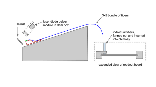
We only have cosmic measurements so far for the prototype and for production fibers of type B. For the others, we have compared their response by injecting light from a pulsed laser diode through the end of the light guide with a type B fiber right next to it. There is a diffuser after the laser to make the beam spot > 5cm in size, to reduce position sensitivity and also the intensity of the pulses. There are variations from fiber to fiber, but here is a semi-quantitative comparison, in arbitrary units normalized to the type B pulse height. All SiPM gains have been equalized first.
- G : 30 - 60
- P : 100 - 200
- R : 10 - 30
- B : 250 - 500
- F : 500 - 800
- S : 700 - 1000
- C : 500 - 900
For any given fiber we get consistent results from one pulser run to the next, but there is some question of exactly how these responses map onto scintillation transmission fraction. So far we have had time to measure only two bundles of production fibers with cosmics, both of them type B, one with pulser responses near the low end and the other near the high end of the range 250 - 500 shown above. Both bundles showed similar cosmic response within the 10% statistical precision of the measurement.
Optical cross talk measurements
Optical cross talk was measured by placing a dark mask with a 2mm x 2mm cutout hole in front of an array of 3x5 fibers. About 20cm from the array is a fast-pulse laser diode with a diffuser in front of it, such that the source size is roughly 3cm in diameter.
For these tests, type B fibers (fused, bent, unpainted) fibers were mounted in the dark box. Measurements were taken with and without paper strips between the rows and columns to guarantee their separation. Without the paper, the fibers were in occasional contact with each other without anything in between, but without significant pressure. In both cases no measurable optical signal was seen in any of the other channels in the array, once the mask had been properly aligned with the illuminated fiber. The pulse height in the illuminated fiber was ~800 channels (60 pixels), while in all of the neighboring fibers the average pulse height was less than 2 channels (0.2 pixels) per pulse. We can only give an upper bound because the signal is lost in the single-pixel dark rate, which is about at the that level. The conclusion is that the optical cross talk is negligible, even without paint.
Summary of results from simulation and bench observations
We have spent many hours visually comparing the light escaping from different types of fibers using a diode in a dark room. We also have written a stand-alone Geant simulations of light propagating in single-clad and double-clad fibers with different surface treatments (paint, air, abrasion, random cracks). Another stand-alone simulation is used to determine the path length distribution of cosmic tracks in our cosmic trigger configuration, to allow us to extract the fiber transmission fraction from measured pixel yields in cosmic runs. Here are some observations.
- Light is escaping all along the fibers, mainly from invisible defects in the structure (little micro cracks, speckles). To leading order they all look the same, including type C which looks especially bright and sparkling along its surface when illuminated from one end in a dark room.
- The edges of the square fiber are distinctly bright, as if light is getting trapped there and escapes preferentially from the corners, or perhaps the defect density is high there.
- Bent fibers are more bright along curved sections than straight, sometimes by a factor 2, not more.
- Painted fibers are more bright than unpainted, perhaps by a factor 2-3, especially in the bend regions.
- Overall it was very difficult to predict light yield ratios seen with the pulser by looking at escaping light visually. Even for fibers with almost no light transmission seen with the pulser, the visual exam seemed similar to others with a large pulser signal in side-by-side comparisons in a dark room.
All of these observations only apply to single-clad fibers. To compare with double-clad we have to rely on simulation. Here are some conclusions from simulation.
- If all of the core and cladding surfaces are perfect, the transmission fraction is huge, like 25%, due to the large refractive index ratio between the core (1.6) and air. This disappears when almost any kind of imperfection is introduced in the outer surface (absorbing layer, abrasion and random defects) and the number quickly drops to the capture fraction implied by the core - cladding n-ratio.
- If the inner core-cladding interface is perfect, the transmission factor is 4.3% no matter what you do to the outer surface - paint, absorbing surface layer, surface abrasion and random defects. Under these conditions, bending has very little effect, only a few percent loss for bend radius down to 5 cm.
- If the inner core-cladding interface is imperfect, it is hyper sensitive to what you do there. Almost any imperfections make the result sensitive to conditions in the outer layers: painted vs. not, surface roughness and absorption.
- Adding a second cladding layer does not increase the capture angle of the transmitted light. That is what I thought it would do, but the simulation shows that the transmitted light after traversing 160cm of fiber is essentially all within the cone set by the ratio of refractive indices of the core and inner cladding, once you include imperfections in the boundary layers.
- The second cladding layer increases the transmission fraction by making it less sensitive to imperfections at the outer surface. Without the outer cladding, any light that escapes the core due to inner interface ripple reaches the outer surface has a good chance of being lost. If there is a second cladding, the light has a much better chance of being reflected back, after which it re-enters the core and is re-trapped inside. So with the second cladding layer, the chance of light loss is 1/N^2 instead of 1/N, where N is the mean number of boundary reflections before light that is nominally trapped inside the core hits a boundary defect and escapes.
This last point explains why we didn't see any loss in yield from the paint with the double-clad light guide fibers that we used in the prototype, but we see this large factor 2 effect now in the production fibers which are single-clad.
